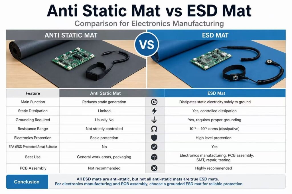
ESD Bench Mat and Workbench Mat: Construction, Resistance and How to Choose One
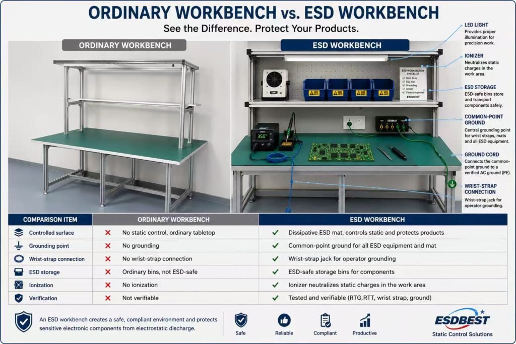
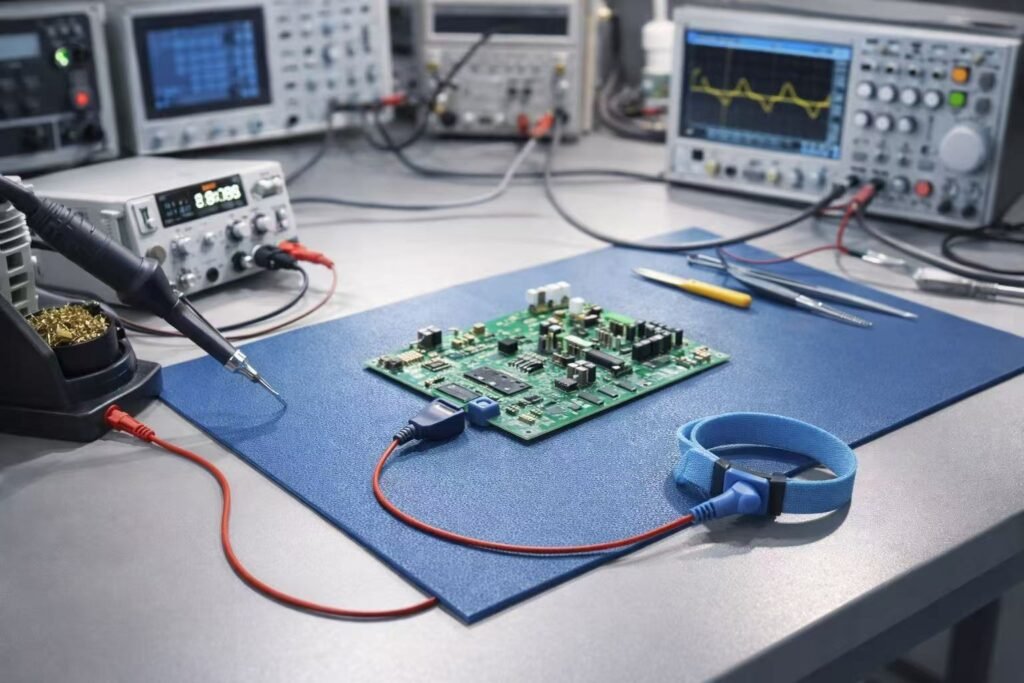
An ESD bench mat is a static-control work surface placed on a workbench to safely dissipate electrostatic charge from tools, components and operators. It works only when it is grounded, and only when its electrical resistance sits within the range specified for static-dissipative work surfaces.
Quick Summary
- What it is: A grounded static-dissipative work surface for electronics handling
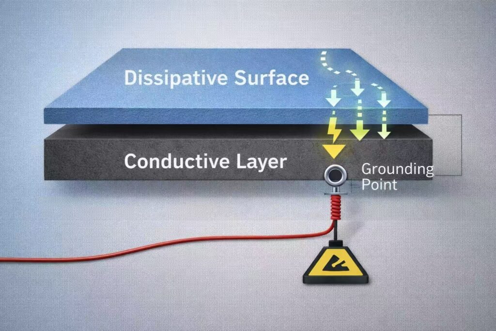
- How it works: A dissipative top layer moves charge in a controlled way to a conductive bottom layer, then to ground
- Typical construction: Two bonded rubber layers, 2 mm or 3 mm total
- Where it is used: PCB assembly, SMT lines, repair benches, laboratories, cleanrooms
- Key requirement: It must be connected to ground, and its resistance must be verified — not assumed
How Does an ESD Bench Mat Work?
An ESD bench mat provides a controlled path to ground so that static charge drains away gradually instead of discharging suddenly into a component.
Charge is generated constantly on a working bench — by friction between packaging and parts, by an operator’s clothing and movement, by tools being picked up and put down. On an insulating surface such as a plain laminate bench top, that charge has nowhere to go. It accumulates until something conductive touches it, and the resulting discharge can damage a device instantly or leave latent damage that only shows up in the field.
An ESD bench mat solves this by being conductive enough to move charge, but resistive enough that the charge does not move too fast. That balance is the entire point of the two-layer construction below.
What Is Inside a Two-Layer ESD Bench Mat?
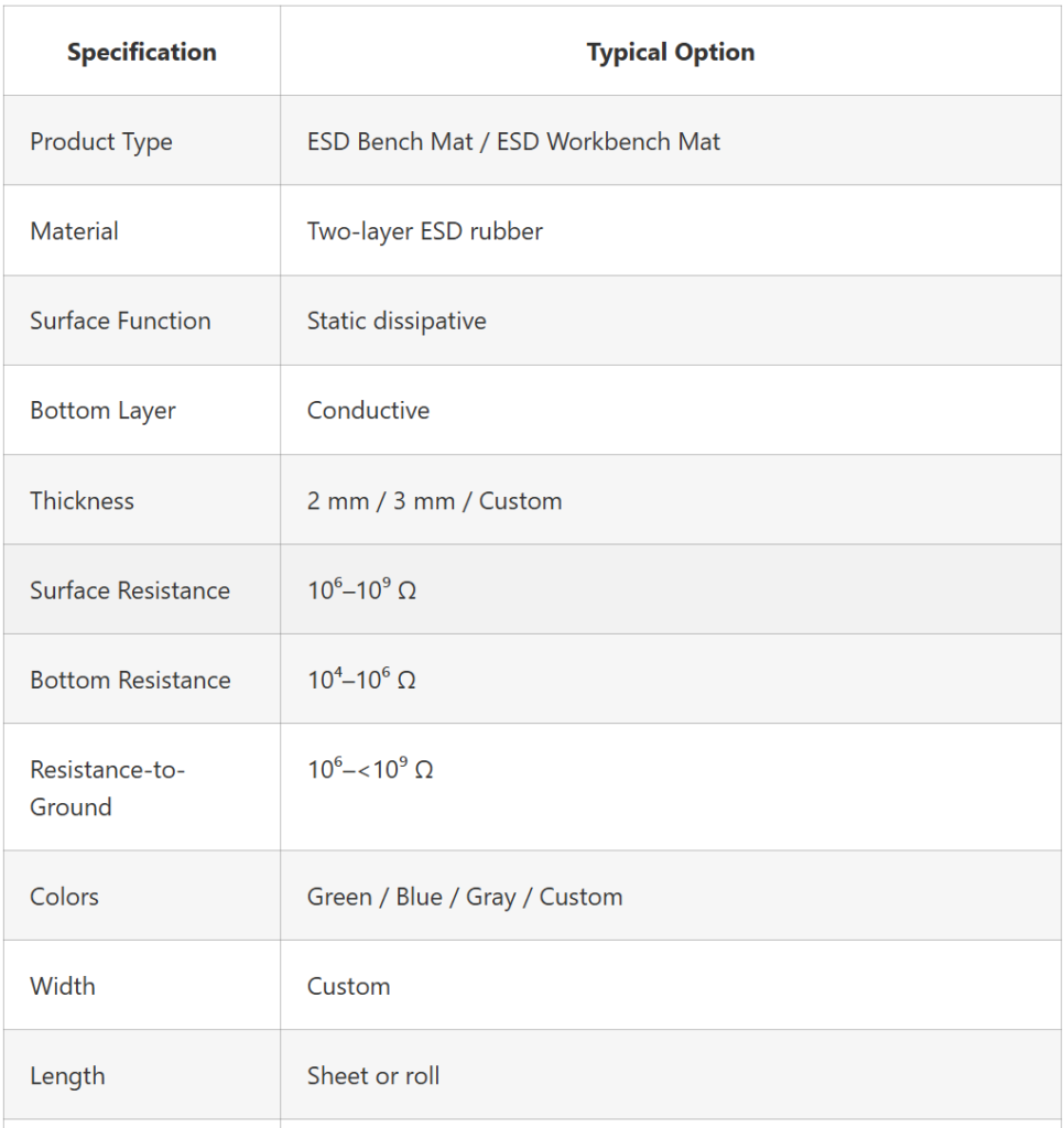
A two-layer rubber ESD bench mat consists of a thin static-dissipative top layer bonded to a thicker conductive bottom layer. The two layers do different jobs and are specified against different resistance ranges
- Green dissipative top layer: the working surface. Specified at 1 × 10⁶ to 1 × 10⁹ Ω. High enough resistance to prevent rapid discharge into a component.
- Black conductive bottom layer: the ground path. Specified at 1 × 10⁴ to 1 × 10⁶ Ω. Low enough resistance to carry charge efficiently to the grounding point.
Because the two layers have different jobs, quoting a single resistance figure for “the mat” describes neither layer accurately. This matters at incoming inspection, and it is the source of the most common testing error we see — covered in our guide on how to test an ESD mat.
Measured Layer Thickness
The following were measured in-house on an ESDBEST 2 mm bench mat sample using a digital caliper, taken at a cut cross-section rather than at a lifted edge.
| Layer | Measured thickness | Function |
|---|---|---|
| Green top layer | 0.51 mm | Static-dissipative working surface |
| Black bottom layer | 1.55 mm | Conductive ground path |
| Total | 2.06 mm | Nominal 2.0 mm |
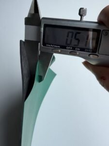

Values are caliper readings on a single sample, not measurements taken under the standardised presser-foot pressure defined in ISO 23529 / ASTM D374. Nominal thickness remains 2.0 mm.
What Resistance Should an ESD Bench Mat Have?
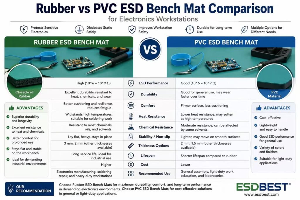
For electronics work, the dissipative working surface should measure between 1 × 10⁶ and 1 × 10⁹ Ω, in line with the worksurface requirements referenced by ANSI/ESD S20.20 and IEC 61340-5-1.
Lower is not better. A surface that is too conductive discharges a component too quickly, which is itself a damage mechanism. A surface that is too resistive holds charge for too long. The dissipative range exists precisely because both extremes cause problems.
If you are still deciding between mat types, see conductive vs dissipative mats.
Measured Point-to-Point Resistance — Actual Test Data
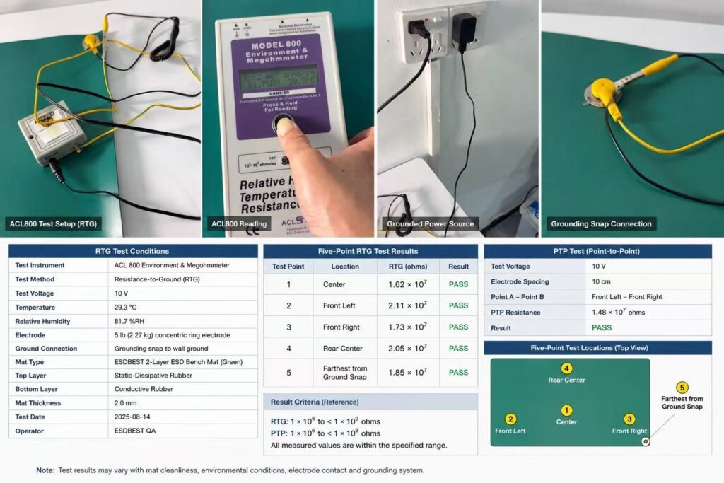
Most suppliers publish only a nominal resistance range. The readings below are actual measurements taken on an ESDBEST bench mat sample, with each layer measured separately against its own specification.
Test conditions
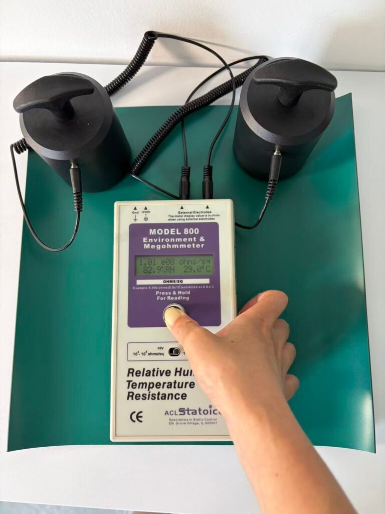
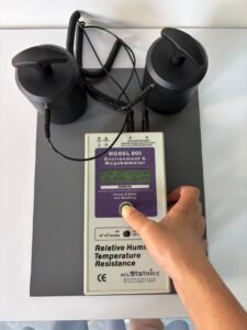
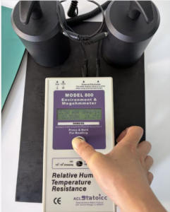
- Instrument: ACL Staticide Model 800 environment and megohmmeter
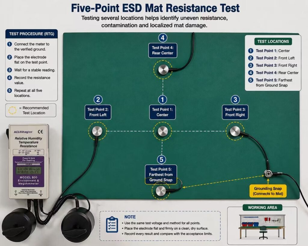
- Method: point-to-point (PTP), two weighted electrodes
- Test voltage: 10 V
- Electrode spacing: 15 cm (150 mm)
- Temperature: 29.2–29.4 °C
- Relative humidity: 81.7–82.5 %RH
- Sample: 25 × 30 cm, 2.0 mm, two-layer rubber bench mat
- Test date: 29 July 2026 | Operator: Ailon Chen
Green dissipative top layer — specification 1 × 10⁶ to 1 × 10⁹ Ω
| ID | Measured PTP resistance | Result |
|---|---|---|
| PTP-T01 | 2.00 × 10⁶ Ω | Within specification |
| PTP-T02 | 2.01 × 10⁶ Ω | Within specification |
Black conductive bottom layer — specification 1 × 10⁴ to 1 × 10⁶ Ω
| ID | Measured PTP resistance | Result |
|---|---|---|
| PTP-B01 | 5.76 × 10⁴ Ω | Within specification |
| PTP-B02 | 3.12 × 10⁵ Ω | Within specification |
| PTP-B03 | 3.12 × 10⁵ Ω | Within specification |
| PTP-B04 | 6.23 × 10⁴ Ω | Within specification |
| PTP-B05 | 6.26 × 10⁴ Ω | Within specification |
| PTP-B06 | 3.50 × 10⁴ Ω | Within specification |
All eight recorded measurements fell within the specified range for the layer being measured. The dissipative surface recorded 2.00–2.01 × 10⁶ Ω; the conductive layer recorded 3.50 × 10⁴ to 3.12 × 10⁵ Ω.
Test evidence
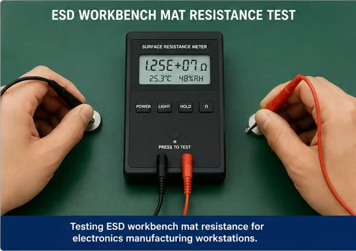
The following photographs were taken during the measurements above. Each shows the reading together with the ambient temperature and relative humidity logged by the instrument at that moment. Surface resistance varies with humidity, so a reading quoted without its ambient conditions cannot be meaningfully compared against a reading taken elsewhere.
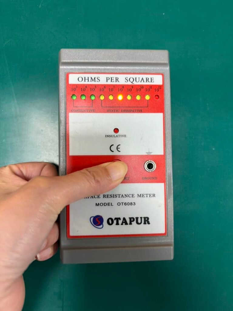
Note that the meter’s display label reads “ohms/sq”; when external electrodes are connected, as here, the displayed value is in ohms.
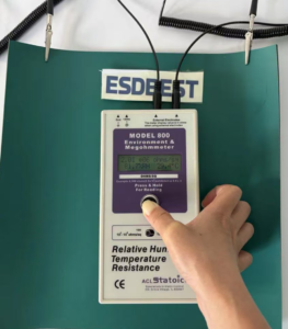
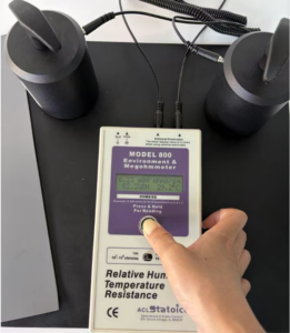
Scope: these values apply to the tested sample under the documented conditions. They are not a substitute for lot-by-lot QC records. Buyers requiring batch-specific verification should request the corresponding QC documentation with their order.
Bench Mat, Workbench Mat, Anti-Static Mat: Are They the Same Thing?
In practice these terms describe the same product. “ESD bench mat” and “ESD workbench mat” are used interchangeably, and “anti-static bench mat” is the older term for the same item. What matters is not the name on the label but the resistance the surface actually measures.
ESD bench mat vs ESD workbench mat
No difference. Both refer to a static-dissipative mat sized for a work surface. “Workbench mat” is more common in production and repair environments; “bench mat” is more common in laboratory and inspection settings. Buyers in different regions default to different terms.
Anti-static vs static-dissipative
This distinction does matter technically. “Anti-static” originally described a material with low charge generation — it resists building up a charge in the first place. “Static-dissipative” describes a defined resistance range that allows an existing charge to bleed away in a controlled way.
Most products sold today as “anti-static bench mats” are in fact static-dissipative mats. If you are specifying a mat for an EPA, ask for the measured resistance range rather than relying on the product name. See conductive vs dissipative mats for the full comparison.
What about “ESD work surface”?
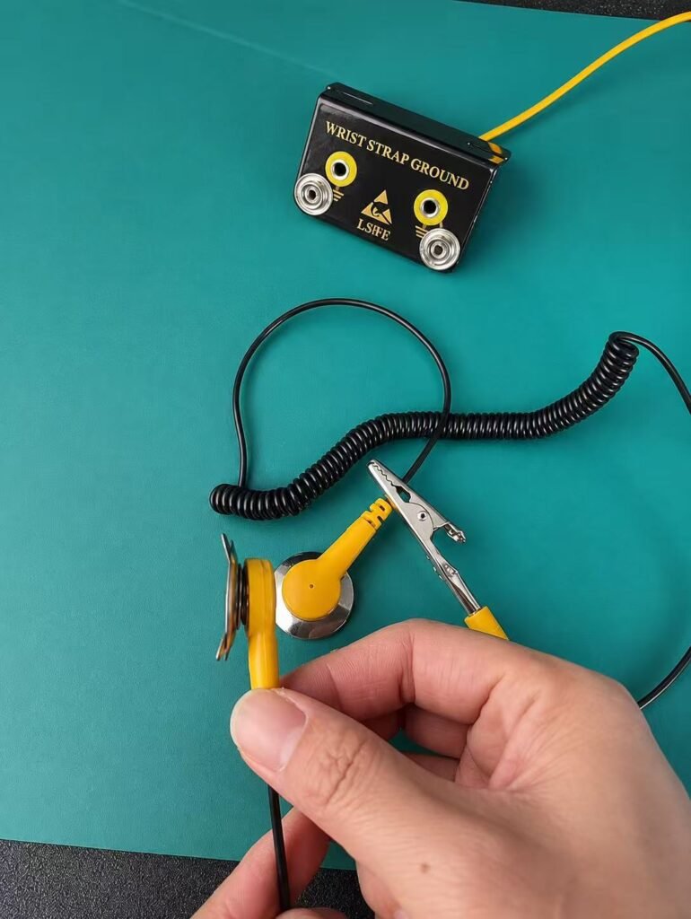
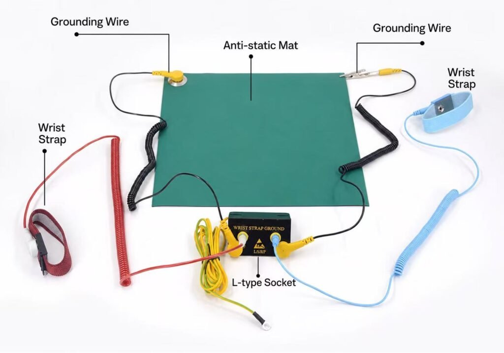
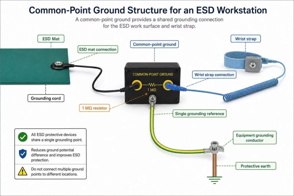
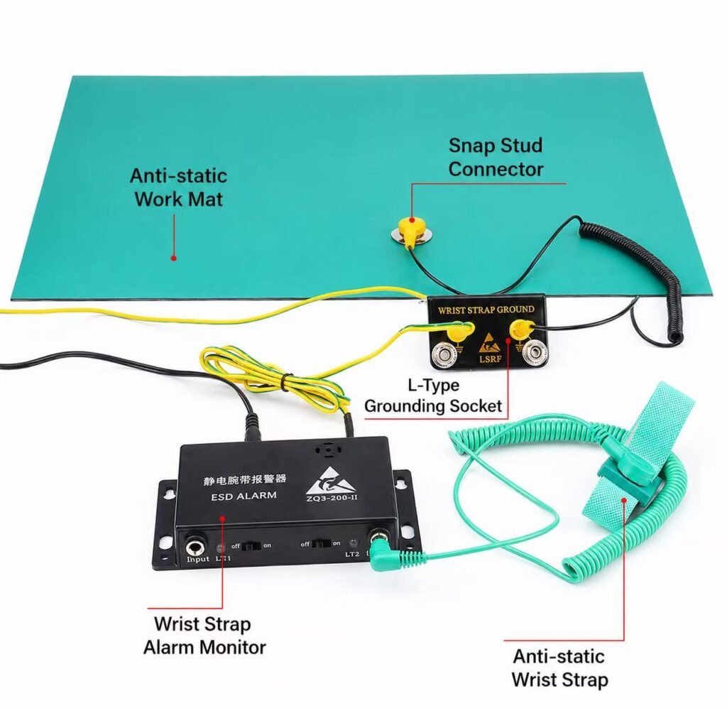
An ESD work surface is the whole grounded bench top, of which the mat is one component. A specification for an ESD work surface covers the mat, the ground cord, the common point ground and the connection to the building’s protective earth — not the mat alone. See grounding an ESD mat.
Should You Choose a 2 mm or 3 mm Bench Mat?
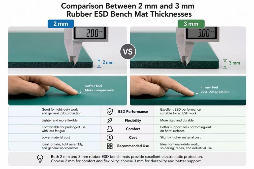
For most bench-top electronics work, 2 mm is sufficient. Choose 3 mm where the bench sees heavier tooling, more impact, or where a softer feel under hand is preferred for long assembly shifts.
Thickness does not change the electrical specification. In a two-layer construction the additional thickness is carried by the conductive bottom layer, while the dissipative working surface stays thin. The working surface is what determines surface resistance, and it is specified by compound, not by how thick the mat is overall.
Both thicknesses are available cut to size or as rolls in 1.0 m and 1.2 m widths — see ESD rubber mat roll sizes, lead time and MOQ.
Common Mistakes to Avoid
- Assuming a mat is grounded because it is installed. A mat with no ground cord, or with a cord clipped to painted metal, is an insulator with a colour. See grounding an ESD mat.
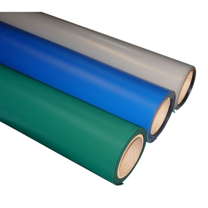
- Judging a mat by colour. Green, blue and grey are cosmetic. Resistance must be measured.
- Comparing both layers against one resistance range. The top and bottom layers have different specifications. Testing the black layer against 10⁶–10⁹ Ω will produce a false failure.
- Buying by product name rather than by measured resistance. “Anti-static” on a label tells you very little.
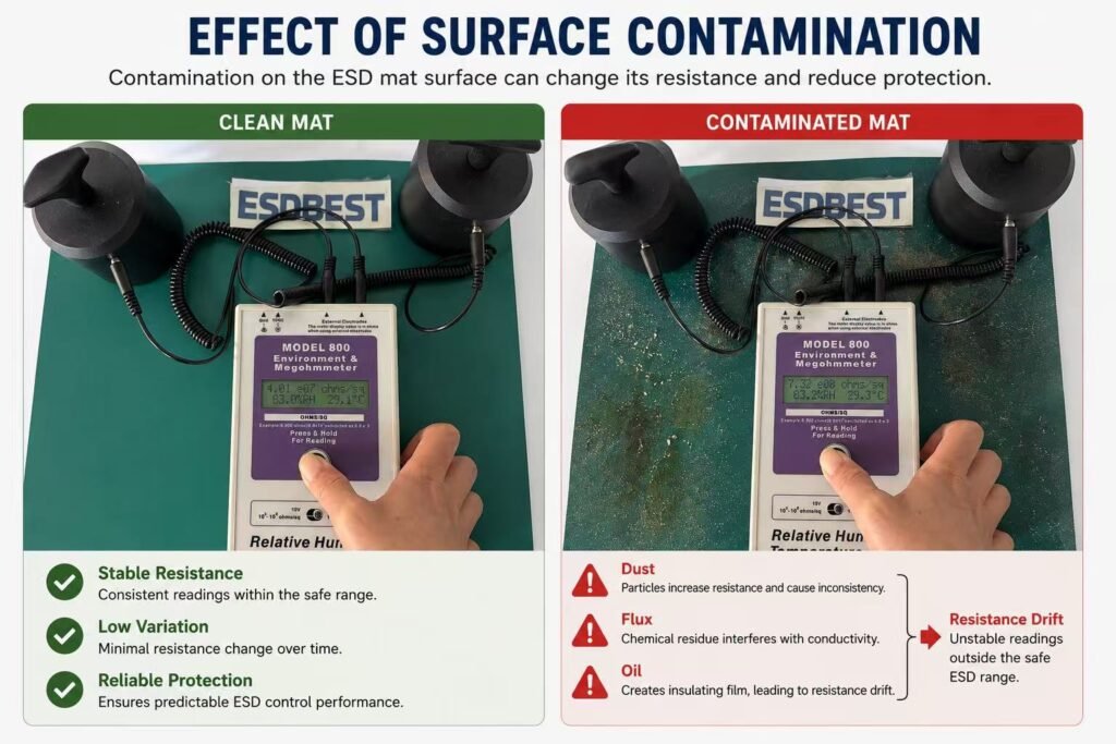
- Cleaning with industrial alcohol or solvent wipes. This changes the surface resistance over time. See how to clean an ESD mat.
- Never re-testing after installation. Resistance drifts with contamination, wear and age. Periodic verification is part of an ESD control programme.
Frequently Asked Questions
What is an ESD bench mat used for?
It provides a grounded, static-dissipative work surface for handling electronic components during assembly, soldering, testing and repair.
Is an ESD workbench mat the same as an ESD bench mat?
Yes. The two terms describe the same product and are used interchangeably.
What is the difference between an anti-static bench mat and an ESD bench mat?
In practice they are sold as the same product. Technically, “anti-static” refers to low charge generation and “static-dissipative” refers to a defined resistance range. Specify by measured resistance rather than by name.
Does an ESD bench mat need to be grounded?
Yes. Without a connection to ground, the mat has no path to discharge to and cannot perform its function.
What resistance should an ESD bench mat have?
The dissipative working surface should measure 1 × 10⁶ to 1 × 10⁹ Ω. The conductive bottom layer is specified separately, typically 1 × 10⁴ to 1 × 10⁶ Ω.
Why does an ESD mat have two layers?
The layers do different jobs. The top layer controls the rate of discharge from the working surface; the bottom layer carries charge efficiently to the grounding point.
Is a thicker ESD mat better?
Not electrically. Thicker mats offer more cushioning and impact resistance, but surface resistance is determined by the compound of the top layer, not by total thickness.
Can I use a normal rubber mat instead?
No. An ordinary rubber mat has uncontrolled resistance and provides no verified discharge path.
How often should an ESD bench mat be tested?
Testing frequency should follow your ESD control programme. Many facilities test on installation and then at regular intervals thereafter.
What sizes are available?
Mats can be supplied cut to size or as rolls in 1.0 m and 1.2 m widths. See ESD rubber mat roll sizes, lead time and MOQ.
Can ESD bench mats be customised?
Yes. Size, colour, surface finish and thickness can be specified for OEM and distributor orders.
What is the difference between an ESD bench mat and an ESD floor mat?
A bench mat protects components at the work surface. A floor mat controls static generated by personnel movement. They are not interchangeable.
Written by Rachel Zhong, HORBEST Tech Co., Ltd. HORBEST has manufactured ESD control products in Shenzhen since 1996, supplying OEM and private-label matting to distributors in Europe, North America, Japan and Southeast Asia. The measurements published on this page were taken in-house. Jinwen Shuzigu, Huangtian, Xixiang, Bao’an, Shenzhen, China. Tel: +86 137 1427 2599