How to Test an ESD Mat: A Step-by-Step Incoming Inspection Method
Updated 20 October 2026 · New measurements taken on 19 October 2026.
To test an ESD mat, use a resistance meter with weighted electrodes to measure point-to-point resistance on the working surface. Then measure from one electrode on that surface to the mat’s groundable point, usually its ground snap. For worksurface product qualification under ANSI/ESD S20.20, both measurements must be below 1 × 10⁹ Ω when tested using the applicable ANSI/ESD STM4.1 procedure.
On a two-layer ESD bench mat, apply the working-surface acceptance criteria to the surface where ESD-sensitive items are placed. The black conductive backing may have a much lower manufacturer-specified resistance range. Testing that backing against a dissipative top-surface specification can cause a false rejection.
This guide explains a practical incoming inspection workflow. For formal product qualification, follow the applicable standard edition and its complete requirements for electrodes, sample preparation, conditioning, voltage selection and measurement time. Routine incoming checks do not replace product qualification.
Quick answer: which limits apply?
| What you measure | Acceptance criterion | Basis |
|---|---|---|
| Working surface, point to point | < 1 × 10⁹ Ω | ANSI/ESD S20.20 worksurface product qualification, using ANSI/ESD STM4.1 |
| Working surface to groundable point | < 1 × 10⁹ Ω | ANSI/ESD S20.20 worksurface product qualification, using ANSI/ESD STM4.1 |
| Installed working surface to ground | < 1 × 10⁹ Ω | Compliance verification under the ESD control programme, using the applicable ESD TR53 procedure |
| Additional lower limit where CDM damage is a concern | Consider ≥ 1 × 10⁶ Ω for point-to-point and point-to-groundable-point resistance | Document the adopted lower limit in your specification and ESD control programme |
| Conductive bottom layer | Use the manufacturer’s separate specification; 1 × 10⁴ to 1 × 10⁶ Ω for the sample discussed here | Product datasheet; not a universal range for every ESD mat |
The 1 × 10⁶ to 1 × 10⁹ Ω window found on many datasheets is a specified range for a dissipative working surface. It should not automatically be applied to every layer of a multi-layer mat. A datasheet also does not override the programme’s strict upper criterion of less than 1 × 10⁹ Ω.
For background, see conductive vs dissipative ESD mats. For product selection, see our ESD mats for workbenches and floors.
Before you start: identify the layers
- Check the datasheet. It should identify the working surface and give a separate specification for the conductive backing where applicable. If only one range is listed, ask the supplier which surface and test method it describes.
- Look at the edge. A two-layer rubber mat commonly has a coloured working surface over a black backing. Confirm the construction with the supplier rather than relying on colour alone.
- Inspect the ground snap. Confirm that the snap is secure and installed as the manufacturer specifies. Its appearance alone does not prove a reliable electrical connection.
- Mark the working surface. Use a small label outside the measurement area so the sample is not tested upside down.
Equipment checklist
- ☐ Resistance meter covering the expected measurement range and supporting the test voltages required by the applicable procedure
- ☐ Two weighted electrodes with conductive rubber contacts that meet the applicable test method
- ☐ Suitable leads and a clip for the mat’s ground snap
- ☐ Clean insulating support that meets the test procedure’s requirements
- ☐ Thermometer and hygrometer, or suitable built-in environmental sensing
- ☐ Current calibration record for the meter
- ☐ Test record identifying the sample, method, electrode arrangement and acceptance limits
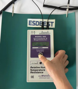
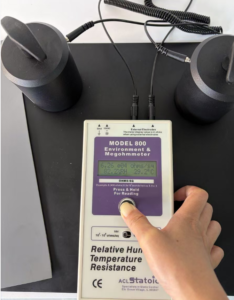
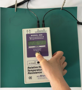
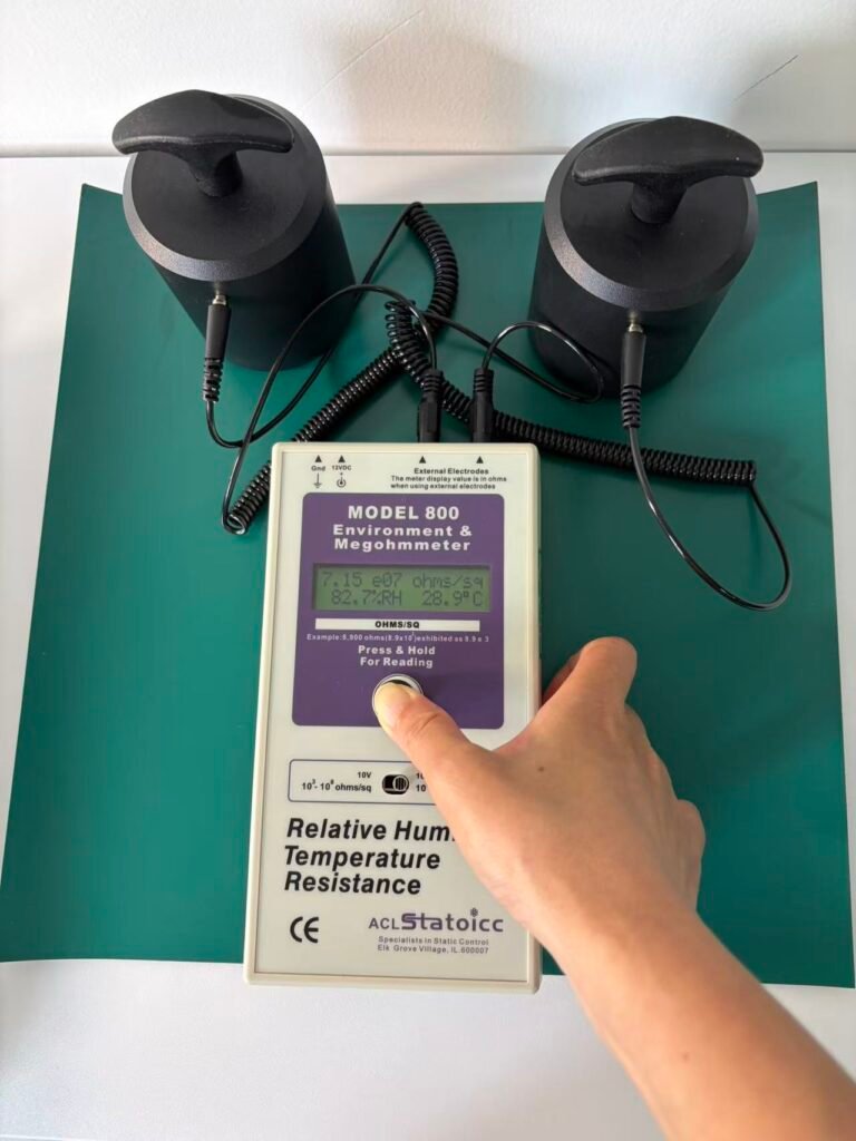
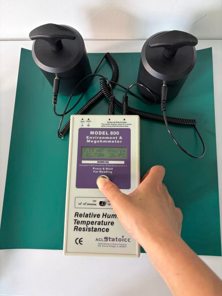
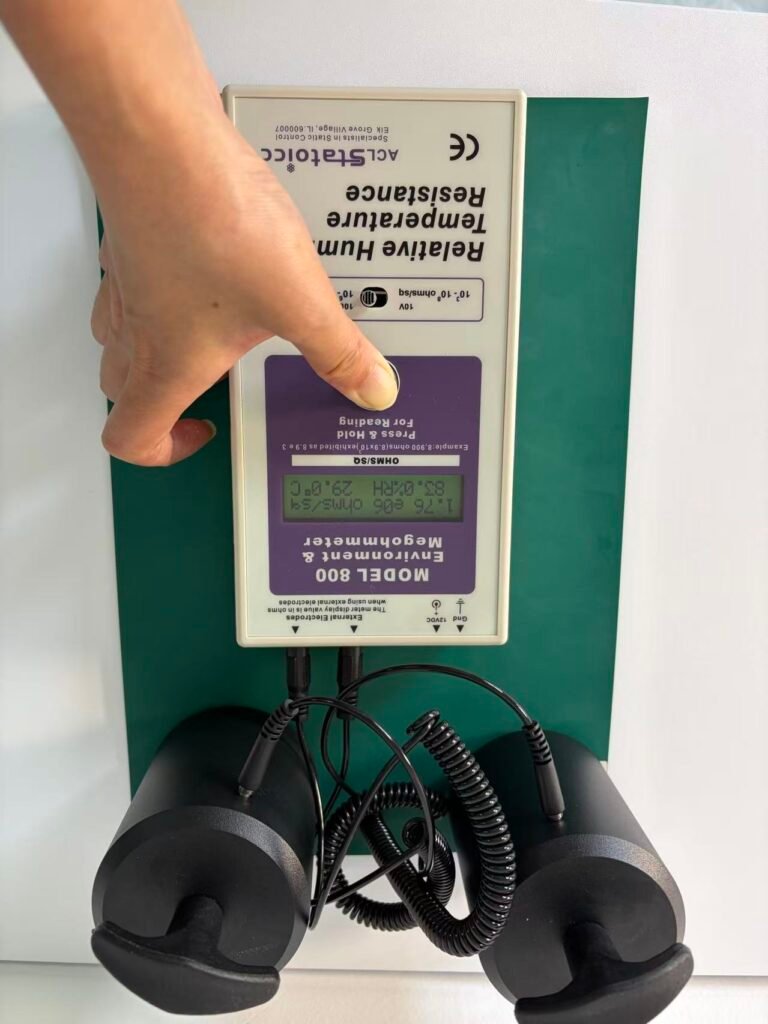
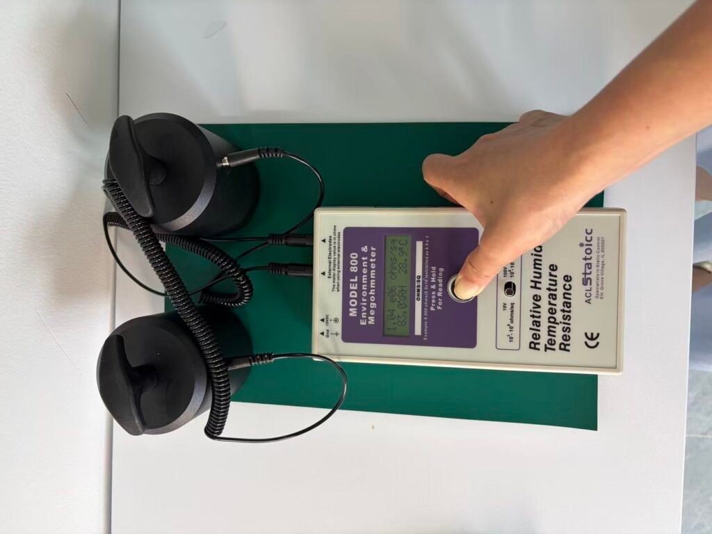
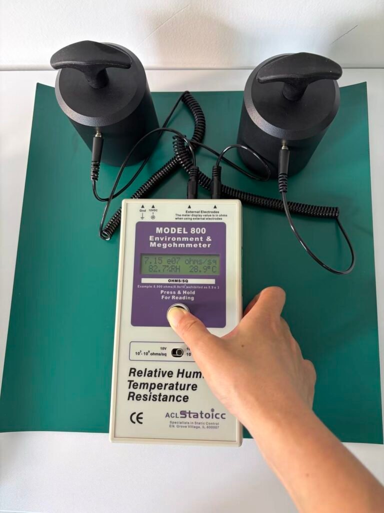
For the measurements reported below, we used an ACL Model 800 resistance meter.
Can you use a multimeter? A typical handheld multimeter is not suitable for qualifying an ESD mat. It usually cannot measure the required high-resistance range using the specified test voltage. A suitable multimeter can help check a disconnected ground cord for continuity or verify its resistor value, but it cannot establish worksurface compliance.
Step 1: point-to-point test on the top surface
- Record the sample condition. Note whether it is being tested as received or after cleaning. If cleaning is part of the agreed procedure, use a manufacturer-approved cleaner and allow the surface to dry fully.
- Prepare the sample. Lay it flat on the specified insulating support, working surface up. Disconnect external grounding connections.
- Position the electrodes. Use the electrode spacing and placement required by your procedure. Keep the arrangement consistent and record it. The measurements reported in this article used a stated spacing of 250 mm.
- Connect the meter. Connect one lead to each electrode using the external electrode connections.
- Select the test voltage. Follow the applicable test method and the instrument instructions. Do not assume that every reading may be taken at 10 V.
- Take the reading. Use the specified electrification time and record the resistance, applied voltage, temperature and relative humidity.
- Repeat across the mat. For the incoming screening checklist below, use at least five agreed electrode positions covering the working area, including positions near the edges. Follow the standard’s sampling requirements for formal qualification.
Acceptance: each result must be below 1 × 10⁹ Ω and meet any additional contractual limits. If your programme adopts a 1 × 10⁶ Ω lower limit, apply that limit as documented.
Step 2: surface-to-groundable-point test
This product-level test measures resistance from the working surface to the mat’s groundable point. It does not include the installed ground cord and the complete connection to ground.
- Keep the sample isolated. Leave the mat on the specified insulating support with external grounding connections disconnected.
- Connect directly to the snap. Attach the return lead directly to the mat’s ground snap or other manufacturer-designated groundable point. Exclude the ground cord and wrist-strap terminal block from this product-level measurement.
- Position one electrode on the top surface. Use the placements and clearances required by the applicable procedure. For incoming screening, include a position near the snap and another far from it.
- Connect the electrode. Connect the electrode to one meter terminal and the snap lead to the other.
- Measure and record. Use the required voltage and electrification time. Record resistance, electrode position, voltage, temperature and humidity.
Acceptance: each result must be below 1 × 10⁹ Ω and meet any additional agreed limits.
A substantially higher result far from the snap is a reason to investigate the sample, snap connection and test setup. The difference alone does not identify a defective conductive layer, and there is no universal near-to-far ratio used here as a pass criterion.
Step 3: optional bottom-layer check
Use this check when the purchase specification includes a separate backing-layer requirement or when you are investigating the mat’s construction. Judge the result against that layer’s datasheet specification.
- Turn the sample over so the conductive backing faces upwards.
- Repeat the point-to-point measurement using the agreed procedure.
- Record the backing-layer results separately from the working-surface results.
For the sample discussed here, the specified backing-layer range is 1 × 10⁴ to 1 × 10⁶ Ω. A result within that range should not be rejected merely because it is below the top surface’s 1 × 10⁶ Ω design minimum.
Learn more about the different roles of conductive and dissipative materials.
What our measurements show
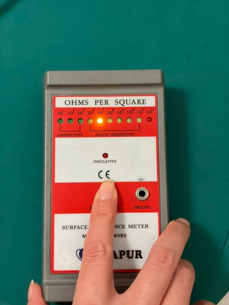
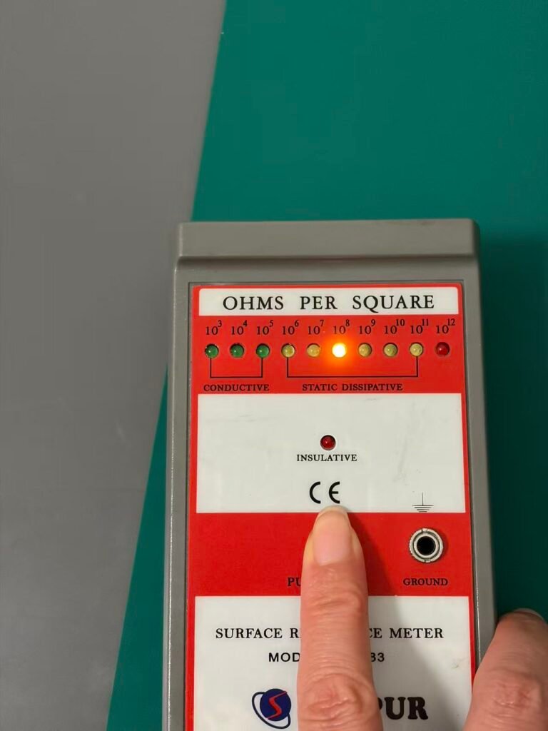
The following in-house measurements were taken on 19 October 2026 on a two-layer rubber bench mat with a green dissipative top and a black conductive backing. The stated setup used an ACL Model 800, a 10 V test range and 250 mm electrode spacing for point-to-point measurements.
| Test | Number of readings | Measured range | Conditions | Observation |
|---|---|---|---|---|
| Top surface, point to point | 9 | 2.26 × 10⁶ to 4.18 × 10⁷ Ω | 65.4–65.7% RH; 29.0–29.8 °C | All recorded values below 1 × 10⁹ Ω |
| Top surface to ground snap | 3 | 1.64 × 10⁷ to 1.99 × 10⁷ Ω | 58.7–58.9% RH; 28.0 °C | All recorded values below 1 × 10⁹ Ω |
| Bottom layer, point to point | 3 | 2.50 × 10⁴ to 4.95 × 10⁴ Ω | 58.1–58.9% RH; 27.9 °C | Within the stated 104–106 Ω backing-layer range |
If the top-surface minimum of 1 × 10⁶ Ω were incorrectly applied to the backing, all three backing readings would be rejected. That would be a mismatch between the tested layer and the acceptance specification.
Scope of these results: the values describe the tested sample under the stated conditions. They are not lot-wide QC records or a complete declaration of conformity. Because these measurements were recorded at 10 V, confirm the voltage-selection requirements of the applicable procedure before using them for formal acceptance or qualification.
Five mistakes that can cause misleading results
- Applying the top-surface range to the bottom layer. Identify the working surface first and use the correct specification for each layer.
- Including extra hardware in a product-level snap measurement. Our reported setup comparisons produced readings of about 2 × 10⁷ Ω with a direct snap connection and 6–10 × 108 Ω through a wrist-strap terminal block. Investigate such differences in the hardware and connections. For installed-system verification, include the intended grounding path.
- Recording the display label without checking the measurement mode. External-electrode resistance measurements are recorded in ohms (Ω). If the display shows “ohms/sq”, confirm the selected mode and the instrument instructions before interpreting the result.
- Omitting temperature and humidity. Environmental conditions can affect resistance. Lower humidity often increases readings, depending on the material. Record the conditions so results can be compared meaningfully.
- Relying on one reading. Use a documented sampling plan that covers the working area. The incoming screening checklist below uses at least five point-to-point positions and two surface-to-snap positions.
Incoming inspection checklist: copy and use
- ☐ Sample ID, supplier, batch and inspection date recorded
- ☐ Working surface and backing layer identified
- ☐ Datasheet states the applicable surface, resistance limits and test method
- ☐ Meter model, serial number and current calibration certificate recorded
- ☐ Electrode specification, condition and spacing recorded
- ☐ Sample preparation and environmental conditioning documented
- ☐ Sample placed on the specified insulating support
- ☐ External grounding disconnected for product-level measurements
- ☐ Test voltage and electrification time follow the applicable procedure
- ☐ Top-surface point-to-point measurements completed at five or more agreed positions
- ☐ Surface-to-snap measurements completed at near and far positions with the return lead connected directly to the snap
- ☐ Working-surface results below 1 × 10⁹ Ω and within any additional agreed limits
- ☐ Optional backing-layer results assessed against their separate specification
- ☐ Resistance, voltage, temperature and humidity recorded for every reading
- ☐ Resistance units recorded as Ω
- ☐ Deviations, retests and final acceptance decision documented
Specification wording you can use
Measure point-to-point resistance and resistance to the groundable point on the designated working surface using the applicable edition of ANSI/ESD STM4.1. Both results shall be less than 1 × 10⁹ Ω. Where the documented ESD control programme requires a CDM-related lower limit, both shall also be at least 1 × 10⁶ Ω.
For the product-level resistance-to-groundable-point measurement, connect the return lead directly to the mat’s designated ground snap or groundable point. Evaluate the conductive backing against its separate contractual specification, where applicable; do not apply the working-surface design minimum to that backing automatically.
Record sample identification, electrode arrangement, preparation and conditioning, test voltage, electrification time, temperature, relative humidity and each resistance result. Verify the installed worksurface-to-ground path separately using the applicable ESD TR53 procedure.
How often should an ESD mat be tested?
Check mats at incoming inspection and after installation, then at the interval documented in your ESD control programme. Set the verification frequency according to device sensitivity, use, contamination, wear and previous results.
Re-test after an event that could change performance, such as a chemical spill, a cleaner change, a damaged snap or visible wear. Follow the manufacturer’s cleaning instructions; see how to clean and maintain an ESD mat.
For an installed mat, measure through the intended grounding path, including the ground cord and common point ground, to the defined ground reference. A direct surface-to-snap measurement alone does not verify that complete path see how the ESD mat ground path works.
For installation details, see how to ground an ESD mat.
Frequently asked questions
What is an ESD mat tester?
An ESD mat tester is a resistance meter used with suitable electrodes and leads to measure resistance across the working surface and from that surface to a groundable point or ground. Select equipment that supports the range and procedure you need.
What resistance should an ESD mat have?
For worksurface product qualification under ANSI/ESD S20.20, point-to-point and point-to-groundable-point resistance must be below 1 × 10⁹ Ω using the applicable test method. Apply any additional lower limit or tighter purchase specification documented for your application.
Is 1 × 10⁶ Ω a required lower limit?
It is not a universal lower acceptance limit for all worksurfaces. A 1 × 10⁶ Ω lower limit should be considered where CDM failures are a concern. If adopted, document how it applies to working-surface point-to-point and point-to-groundable-point measurements.
Why does my mat read 104 Ω?
You may be measuring a conductive backing, but first check the surface, instrument mode and connections. A reading near 104 Ω can be expected for some conductive layers. Compare it with the specification for the surface actually being tested.
How do I check ESD mat grounding with a multimeter?
A suitable multimeter can help check a disconnected ground cord for continuity and measure its resistor, if fitted and within the meter’s range. Use an appropriate resistance meter and electrode to evaluate the mat’s working surface and the installed path to ground. Do not use a resistance measurement to establish the safety of a mains protective-earth connection.
What is the difference between point-to-point and resistance-to-ground testing?
Point-to-point testing measures resistance between two electrodes on the working surface. Product-level point-to-groundable-point testing measures from that surface to the mat’s snap. Installed resistance-to-ground testing includes the intended connection from the surface through the grounding system to ground.
Does humidity affect ESD mat resistance?
Yes. The effect depends on the material, but resistance often rises as humidity falls. Record temperature and humidity and follow the conditioning requirements of your test procedure.
Do I need a calibrated instrument?
Use equipment with a current calibration status appropriate to your quality system and test procedure. Record the meter’s identification and calibration certificate, and inspect the electrodes and leads before testing.
Need help specifying a two-layer ESD bench mat?
Explore our two-layer ESD bench mats, or request a factory quote. Include your required size, thickness, working-surface resistance range, grounding arrangement and inspection method so the quotation and acceptance criteria describe the same product.
About the author. Rachel Zhong is an ESD engineer with 29 years’ experience in static-control materials. The in-house measurements reported here used an ACL Model 800. The supplied calibration record is certificate 1245/617, dated 19 August 2026.
References. ANSI/ESD S20.20; ANSI/ESD STM4.1; ESD TR53. Use the editions specified by your ESD control programme or customer contract. Standards and technical resources are available from the EOS/ESD Association.
Quick answer: which limits apply?
| Top surface, point to point | < 1 × 10⁹ Ω | ANSI/ESD S20.20, Table 3 (method ANSI/ESD S4.1) |
| Top surface to ground snap | < 1 × 10⁹ Ω | ANSI/ESD S20.20, Table 3 |
| Installed mat to ground (audit) | < 1 × 10⁹ Ω | ESD TR53, via S20.20 |
| Lower limit 1 × 10⁶ Ω | Optional, recommended where CDM damage is a risk | S20.20 footnote 10 |
| Black conductive bottom layer | No S20.20 requirement; manufacturer design range, typically 1 × 10⁴ to 1 × 10⁶ Ω | Product datasheet |
The 1 × 10⁶ to 1 × 10⁹ Ω window seen on many datasheets, including ours, is a design range for the dissipative top surface. It is not a single limit for the whole mat.
Written by Rachel Zhong, HORBEST Tech Co., Ltd. HORBEST has manufactured ESD control products in Shenzhen since 1996, supplying OEM and private-label matting to distributors in Europe, North America, Japan and Southeast Asia. The measurements published on this page were taken in-house. Jinwen Shuzigu, Huangtian, Xixiang, Bao’an, Shenzhen, China. Tel: +86 137 1427 2599
Download the full PTP test report (PDF) — Report ID ESDBEST-PTP-2026-0729-01, 29 July 2026.
Download the Full PTP Resistance Test Report
Need ESD Grounding Mats for Your Factory?
ESDBEST supplies grounded ESD mats, ESD bench mats, ESD floor mats, grounding cords, and complete ESD workstation solutions for electronics manufacturing.
Email: sales2@esdbest.com
Contact ESDBEST