Our Two-Layer ESD Mat Study Is Published in the ESD Journal
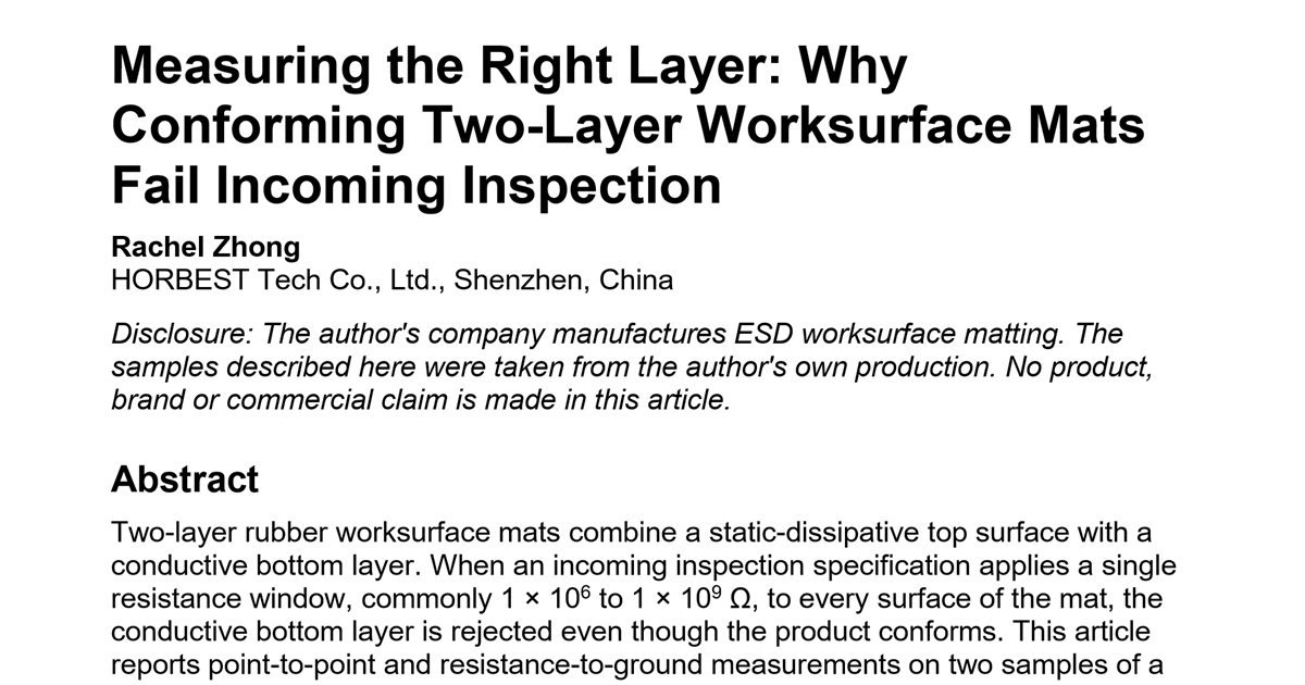
An article by our ESD engineer, Rachel Zhong, is now published on ESDJournal.com, the ESD Journal hosted by EOS/ESD Association, Inc. The article is called Measuring the Right Layer: Why Conforming Two-Layer Worksurface Mats Fail Incoming Inspection. It uses measured data to explain why two-layer ESD mats that meet ANSI/ESD S20.20 can still be rejected at incoming inspection, and how a few lines in a specification prevent it.
Title: Measuring the Right Layer: Why Conforming Two-Layer Worksurface Mats Fail Incoming Inspection
Author: Rachel Zhong, ESD engineer, HORBEST Tech Co., Ltd. (ESDBEST), 29 years in static-control materials
Published: ESD Journal (ESDJournal.com, EOS/ESD Association, Inc.), November 2026
Read it: full article (PDF, 6 pages) · ESD Journal listing
The problem the article looks at
A two-layer rubber ESD mat has two layers, and each one has its own job. The top surface is static dissipative (design range 106 to 109 Ω) and is where ESD-sensitive parts are placed. The bottom layer is conductive (104 to 106 Ω) and carries charge across the mat to the ground snap.
Many incoming inspection specifications give one resistance window, often 1 × 10⁶ to 1 × 10⁹ Ω, without saying which surface it applies to. If an inspector measures the bottom layer or a cut edge, the conductive layer reads "too low" and a mat that conforms is rejected.
What the measurements showed
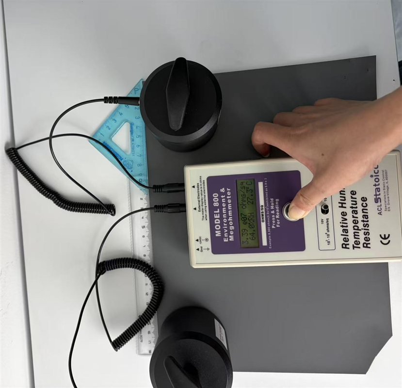
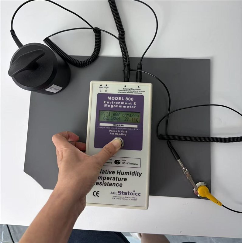
Two samples were measured with a calibrated ACL Staticide Model 800 megohmmeter, with 5 lb weighted electrodes and temperature and humidity recorded for every reading:
| Measurement | Measured range | Against a single 106–109 Ω window |
|---|---|---|
| Top surface, point to point | 2.26 × 10⁶ to 4.18 × 10⁷ Ω | Pass, 12 of 12 readings |
| Bottom layer, point to point | 2.50 × 10⁴ to 2.22 × 10⁵ Ω | "Fail", 8 of 8 readings, although this is the conductive layer's design range |
| Resistance to ground from the top surface | 1.64 × 10⁷ to 2.46 × 10⁷ Ω | About 40–60 times below the S20.20 limit of 1 × 10⁹ Ω |
The same mats passed every reading on the correct surface and failed every reading on the wrong one. The low bottom-layer values are also the reason resistance to ground hardly changed across the mat: on Sample B, four corners read within about 6 % of each other. A mat rejected for those readings is being rejected for the feature that makes it work.

What this means if you write or use a mat specification
- Name the surface. Point-to-point and resistance-to-ground limits apply to the surface on which ESD-sensitive items are placed.
- Treat the bottom layer separately. Either give it its own range (for example 104 to 106 Ω) or leave it out of acceptance testing.
- Be clear about the lower limit. ANSI/ESD S20.20 requires only < 1 × 10⁹ Ω. A 1 × 10⁶ Ω lower limit is an optional choice where CDM damage is a concern, and it applies to the top surface.
- Define the return path. For product acceptance, clip the meter lead directly to the mat's ground snap. Extra ground hardware in the path changed readings by 30 to 60 times in this study.
- Record ohms, not ohms per square. With external electrodes, some meters still show "Ω/sq" on the display. That label is not the quantity you measured.
The full step-by-step method, an inspection checklist and specification wording you can copy are on our page How to Test an ESD Mat.
About the author
Rachel Zhong is an ESD engineer at HORBEST Tech Co., Ltd. (ESDBEST), Shenzhen, with 29 years of experience in static-control materials, including worksurface and flooring compounds, test methods and support for customers' incoming inspection. Contact: sales2@esdbest.com.
The samples in the study came from our own production, as the article discloses. Publication on ESDJournal.com does not mean EOS/ESD Association, Inc. endorses any product.
Need two-layer rubber ESD mats, or help writing an incoming inspection spec your supplier and your QA team both agree on? See our ESD mats and ESD bench mats, or contact us for samples and test data.